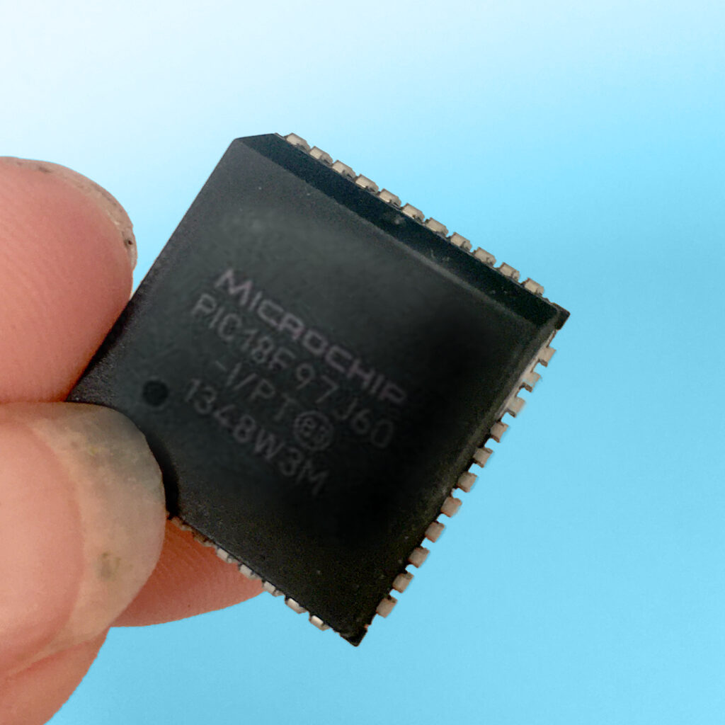
<

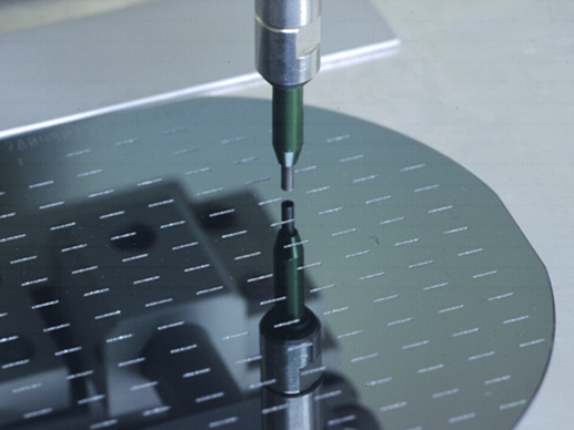
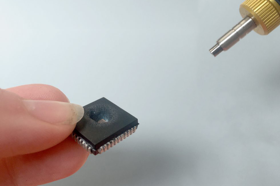
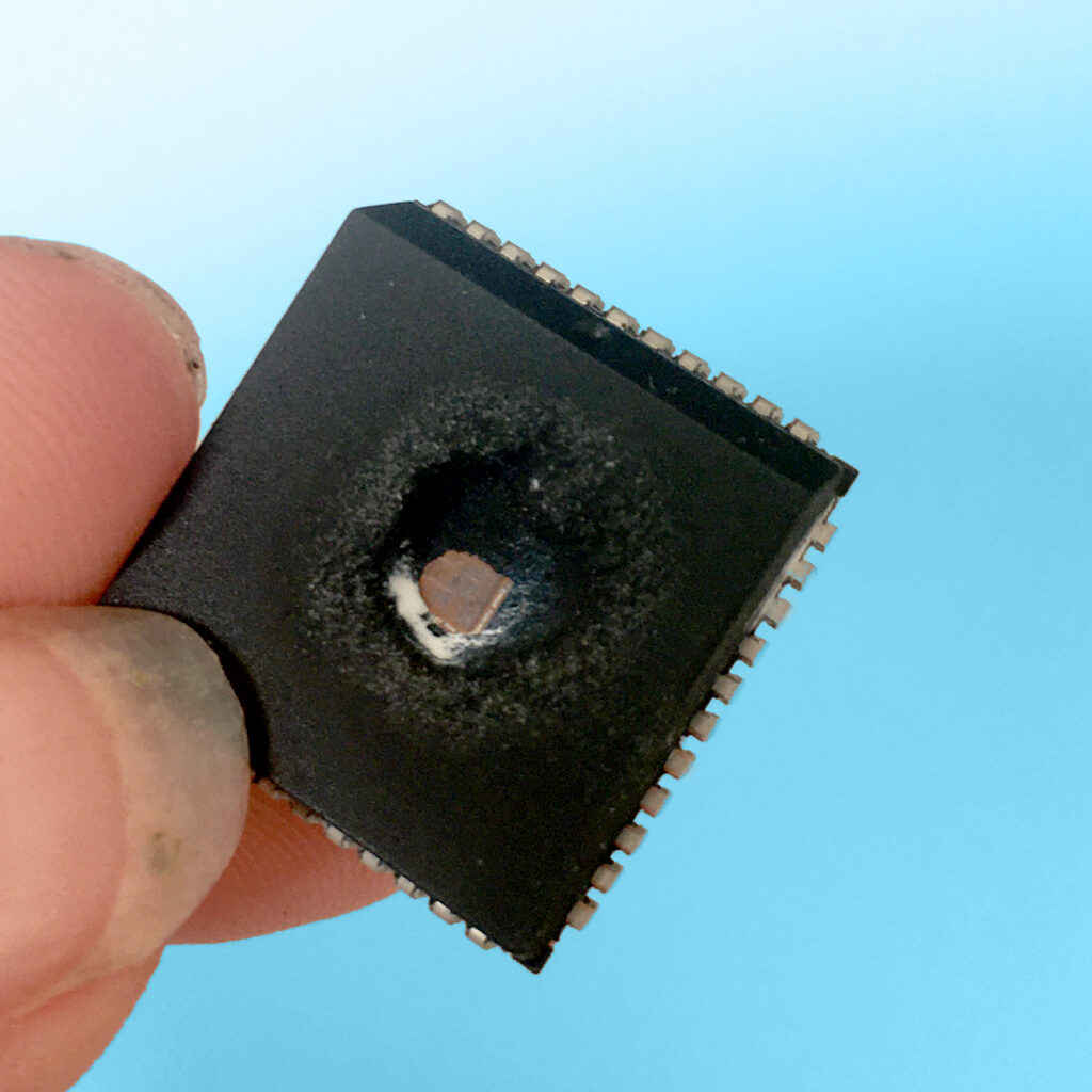
Delicate silicon dies are encapsulated in epoxy to protect them. This becomes a problem when extracting the silicon die for failure analysis or reverse engineering. When using MicroBlasting, decapping an integrated circuit is safer, easier and more environmentally friendly than other methods.

Fine abrasive particles moving at high velocities with a precision nozzle keep the area of removal small. Sodium bicarbonate works well for applications with two layers of different material (like this one) because it’s aggressive against ductile epoxy, but won’t damage harder ceramic. This reduces the risk of cutting the silicon die.

Parameters

  • Abrasive: 50μ Sodium Bicarbonate
  • Pressure: 120 psi
  • Nozzle: 0.046″ Hi/Performance

Before Blasting

After Blasting

Static Protection

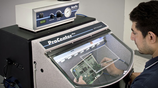
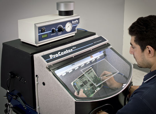
Dry air and abrasive might seem like a hazardous environment for semiconductor devices. This isn’t the case. Our ESD Control ProCenter Plus™ eliminates the potential for static arcing on sensitive components.

The Manual System features the AccuFlo and the ProCenter Plus.
Remove conformal coatings and rework circuit boards with MicroBlasting.

Static Sensitive Applications

We’ve adapted our compact and efficient all-in-one blasting center for static sensitive applications. Continue Reading →

Level Up Your Process

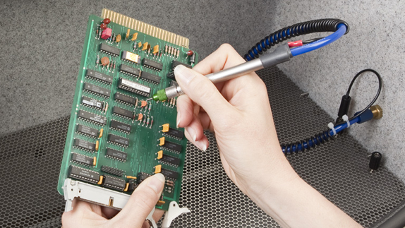
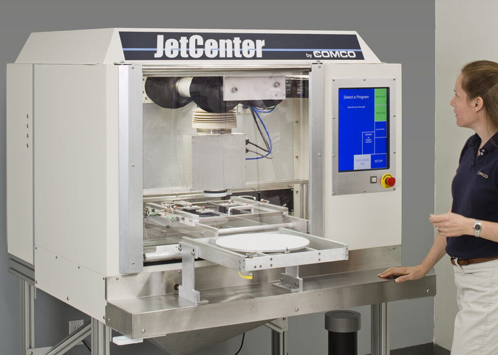
Don’t be afraid to try and automate a static sensitive application. Our JetCenter can incorporate the same ESD protection devices as our ProCenter Plus™.

If you have other unique concerns for your application, contact us! Each automated system is built for your specific application.  Read more about the solutions our engineers have found for challenging applications.


Wafer processing in the Comco JetCenter automated MicroBlasting system

Dig Deeper

Power up and down correctly to prevent abrasive contamination.

Automated MicroBlasting Systems

When a manual MicroBlasting system cannot provide the output or meet your tolerance requirements, Comco’s automated systems deliver. Continue Reading →
Conformal coating removal from circuit board using micro-precision sandblasting.

Conformal Coating Removal with MicroBlasting

Start by blasting from a shallow angle to get the abrasive stream under the surface layer of coating. Essentially “peel” up the coating with the blast stream. Continue Reading →
Processing semiconductor wafers by microblasting slots in the wafer

Semiconductor Processing and Ceramic Machining Using MicroBlasting

MicroBlasting is the ideal method for cutting slots, holes, and apertures in thin, fragile substrates. It is a shockless system that does not generate heat into the wafer, preventing crack formation. Continue Reading →
The Manual System features the AccuFlo and the ProCenter Plus.

The ProCenter Plus

It creates a clean, comfortable work environment with great visibility and is the perfect partner to our AccuFlo. Continue Reading →
Pat B, Sales and Marketing Manager

Questions about MicroBlasting?

Email me or give me a call at 818-841-5500.